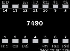
The 7490 is a classic integrated circuit designed as a decade counter. Its primary function is straightforward: it counts from zero to nine in a continuous loop. This cyclic behavior is its default state, making it a staple in digital logic projects where simple base-10 counting is required.
At the hardware level, the output consists of four pins: QA, QB, QC, and QD. These represent a 4-bit binary number. While binary typically counts up to 15 with four bits, the 7490 is hardwired to stop at 9 and reset, effectively creating a decimal counter.
How the 7490 Pinout Outputs Data
To understand the counting sequence, you have to look at the binary representation on the output pins. The pins do not count in standard decimal order; they count in binary, but only display the values for digits 0 through 9.
Here is the exact sequence of states you will see on the QA, QB, QC, and QD pins as the counter increments:
| Decimal Count | QD | QC | QB | QA |
|---|---|---|---|---|
| 0 | 0 | 0 | 0 | 0 |
| 1 | 0 | 0 | 0 | 1 |
| 2 | 0 | 0 | 1 | 0 |
| 3 | 0 | 0 | 1 | 1 |
| 4 | 0 | 1 | 0 | 0 |
| 5 | 0 | 1 | 0 | 1 |
| 6 | 0 | 1 | 1 | 0 |
| 7 | 0 | 1 | 1 | 1 |
| 8 | 1 | 0 | 0 | 0 |
| 9 | 1 | 0 | 0 | 1 |
Notice the pattern? It mirrors standard binary counting for the first ten numbers. Once it hits 9 (1001 in binary), the next clock pulse resets the counter back to 0, rather than proceeding to 10 (1010 in binary).
Why This Matters for Digital Projects
You might wonder why you would use a dedicated decade counter when a microcontroller can handle this easily. The answer lies in simplicity and hardware efficiency. If you are building a digital clock, a scoreboard, or a simple timer without a complex processor, the 7490 does the heavy lifting with minimal external components.
Understanding this pinout is essential for interfacing the chip with seven-segment displays. Each pin drives a specific bit of the binary code needed to decode the number. If your wiring is off, you won’t just see wrong numbers; you’ll see glitches or completely scrambled outputs because the binary weights (1, 2, 4, 8) assigned to QA, QB, QC, and QD won’t match the decoder’s expectations.
For example, QA is the least significant bit (1s place), while QD is the most significant bit in this specific sequence (the 8s place). Getting these connections right ensures that when
The standard decade counter behavior isn’t a hard rule. You can force the chip to reset at arbitrary points. It’s not magic. It’s just wiring.
The mechanism is simple. You manipulate the R01, R02, R91, and R92 lines. Think of these as the chip’s reset triggers.
Here is the logic:
– If R01 and R02 are both high (5 volts).
– And either R91 or R92 is low (ground).
– The chip slams QA, QB, QC, and QD back to zero.
Alternatively, if both R91 and R92 are high. The counter jumps to binary 1001 (decimal 5). This creates a different kind of loop. It doesn’t count to nine. It stops at five.
Building a divide-by-10 counter
You likely already have this one configured. But let’s look at the pins to be sure. Power the chip first. Pin 5 to +5V. Pin 10 to ground.
Now for the control lines. Connect pin 12 to pin 1. This ties the R01 line to ground? No, wait. Let’s be precise.
To get a standard ten-step count (0 through 9):
– Ground pins 2 and 3. These correspond to R01 and R02.
– Leave R91 and R92 alone? No. The text specifies grounding specific pins.
Let’s follow the instructions exactly.
1. Power: Pin 5 (+5V), Pin 10 (Ground).
2. Connect Pin 12 to Pin 1.
3. Ground Pins 2, 3, 6, and 7.
4. Input clock on Pin 14.
The outputs are on QA through QD. You’ll see them on pins 3, 2, 1, and 11? No, QA is pin 3, QB is pin 2, QC is pin 1, QD is pin 11.
“Use the output on pin 11 to connect to the next stage.”
That’s QD. When the counter hits state 9 (1001), the reset condition triggers? Actually, if you ground R01/R02, it resets on the first pulse after 9? No. If R01 and R02 are grounded (low), the reset condition (high/high on R01/R02) is never met.
Wait, let’s re-read the source logic.
“If both R01 and R02 are 1 (5 volts) and either R91 or R92 are 0 (ground), then the chip will reset…”
In the divide-by-10 example:
– Pin 12 (R01) is connected to Pin 1 (QD).
– Pin 10 is ground (Vss).
– Pin 5 is Vdd.
– Pins 2 (R02), 3 (R92?), 6, 7 are grounded.
Actually, the pinout for the 4017 is: